Adding an RGB switch to my TV

Posted by pulkomandy on Thu Oct 26 13:07:55 2023  •  Comments (0)  • 

I have a flat screen TV I bought in 2009. I use it for various retro computer things, mainly when I'm travelling and don't want to carry a CRT around. It is also useful because the VGA port will accept any timing, down to the 18KHz refresh rate of MDA/Hercules at least. It also has a few other cool things my CRTs will not do, like Teletext support.

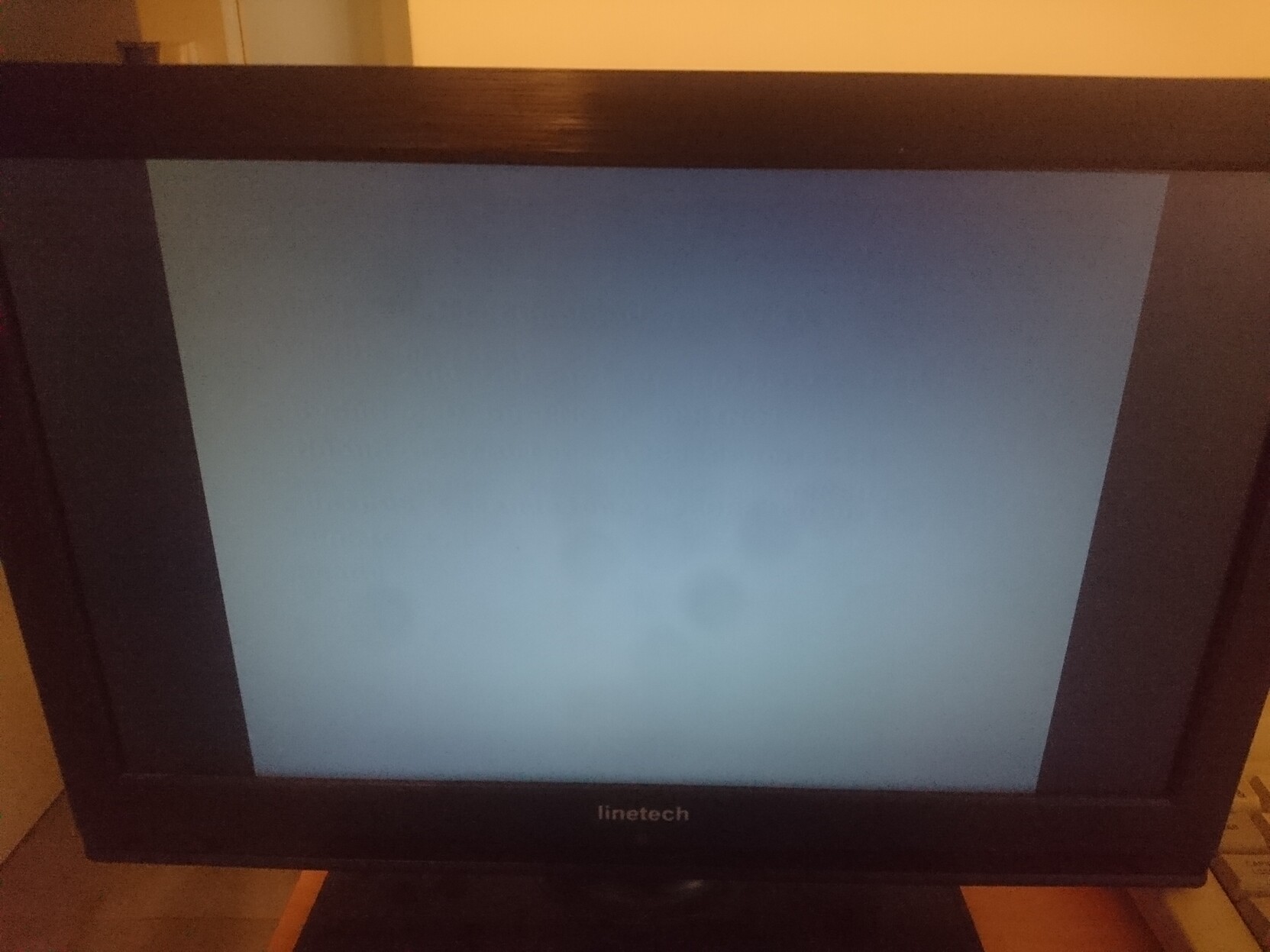
There is just one problem with it, however: there is no way in the menus to force the SCART connector into RGB mode. This can be done only by sending the proper voltage (1 to 3 volts) to the SCART connector itself. Normally this isn't a problem: proper RGB SCART things will send that voltage, and everything will be fine. But I also want to use this port for other stuff, where I make an adapter myself for some other type of RGB output. Often there isn't a voltage source available on the power connector then. As a result, the TV switches to composite mode and shows a grey screen (since it uses the sync signal as a video signal, and so there is nothing to show).

TV showing a grey screen

Previously I did this as an external mod: getting 5V from the USB port of the TV, and feeding back into the SCART. But this requires making SCART connectors with a 5V input, the cable can break when transporting the TV... well, it's annoying. So I decided to make it internally instead.

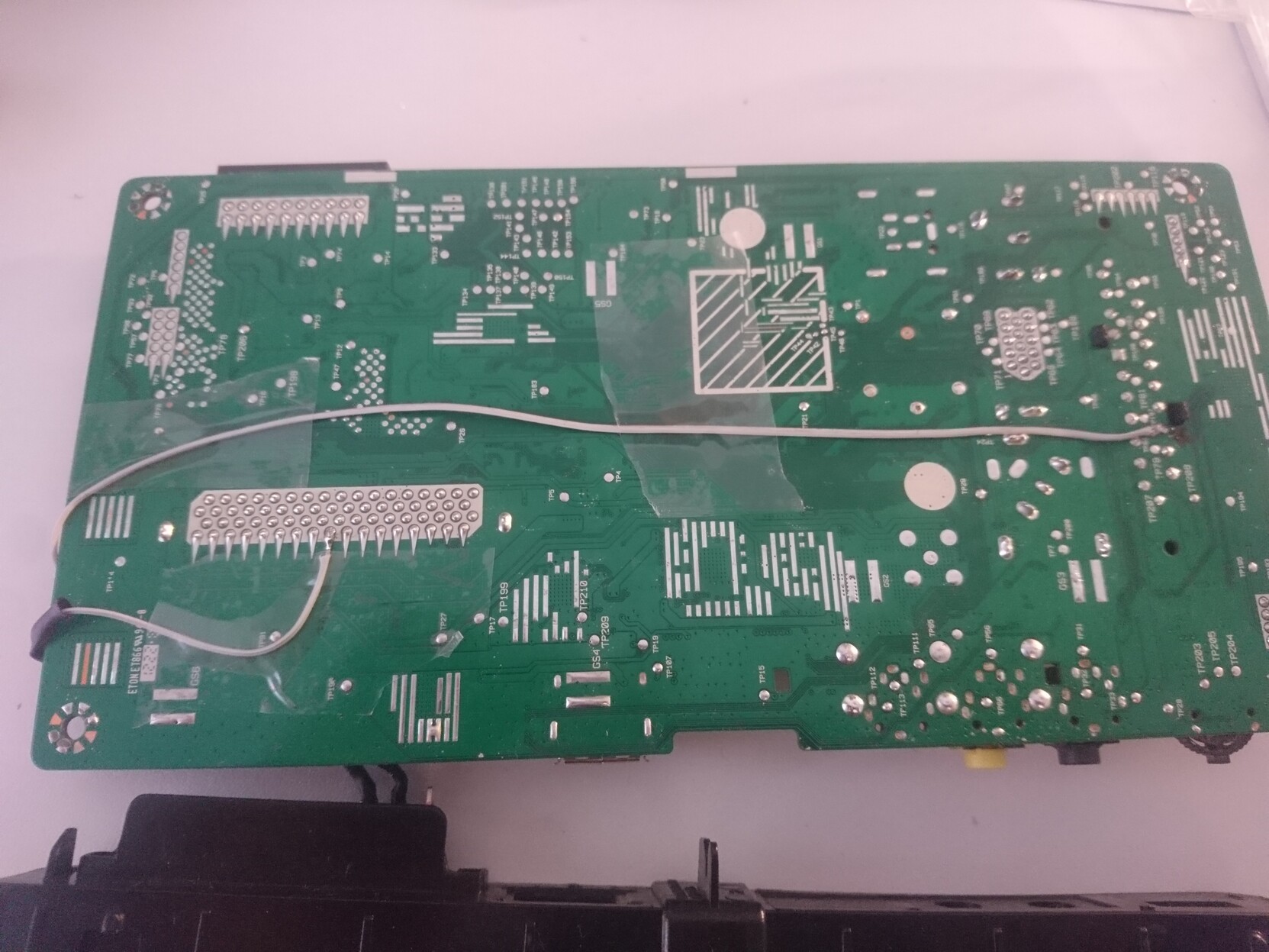
I get the 5V from the Common Interface slot, this is a PCMCIA slot where you could plug a satellite TV receiver or crypted TV decoder or the like. Since this has a standard pinout, the 5V was easy to locate, and also they made it with very large soldering pads so adding a wire there was very easy.

Since the TV expects 1 to 3V on the RGB switching line, I use a 220 ohm resistor. The TV has a 75 ohm impedance, so this creates a voltage divider in the right range. Any resistor from 50 to 300 ohms would do.

Two wires soldered on the PCB, going from CI slot pin 17 to a switch (not visible, on the back of the PCB) and then to SCART pin 16

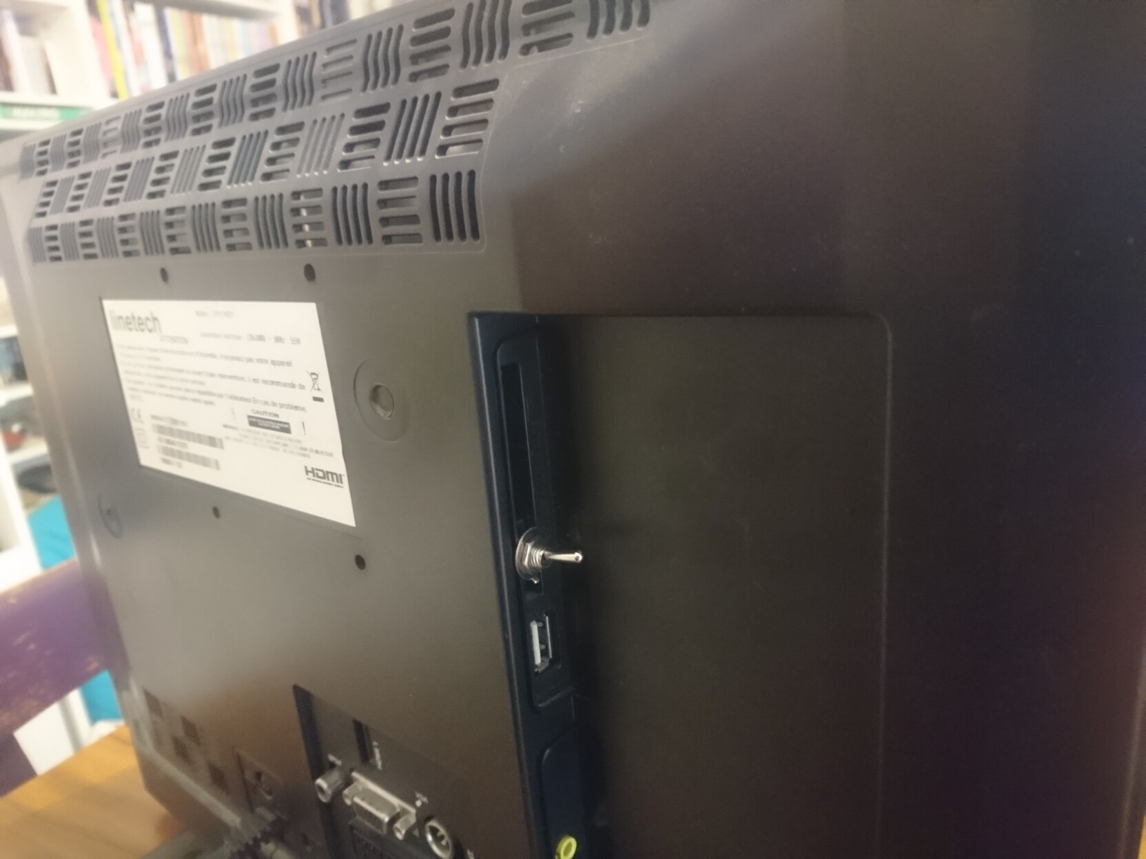
Finally, I mounted the switch by screwing it into the Common Interface slot. The slot is just wide enough to put the switch through, and will provide enough mechanical support once the switch is secured there.

the switch on the back of the reassembled TV

When the switch is ON, this will force the TV to use RGB input on the SCART port. When it's off, the TV will work as normal since the mod is disconnected. A quite simple change in the end, but very useful for me.

A deep dive into Thomson EFCIS graphic controllers

Posted by pulkomandy on Sat Sep 23 22:03:50 2023  •  Comments (0)  • 

So, this week I thought about Thomson EFCIS graphic controllers again. I know that Thomson made at least two families of controllers, the EF934x, which runs the Minitel, and the EF936x, which is designed for pixel graphics, but I did not know as much about this one. It seems a bit more of a "high end" thing, but at the same time, it is loosely similar to the display system used in Thomson TO and MO microcomputers.

I also knew that Thomson EFCIS sold the color palette circuit originally developped for the TO9 as a general color palette chip (the TO9 has it described as a custom chip in its technical manual, but then it became an off the shelf chip).

Anyway, I became curious about the other chips and why and how they were designed. And then I read a lot of datasheets and research papers and patents. Here is what I found.

Note: this is based on some random web searches, I wasn't there at the time (in fact I wasn't born at the time) and I could be misunderstanding or misremembering what I read. Don't trust me too much...

What are we talking about, anyways?

EFCIS is a French semiconductor company. It was created by a public research lab which turned part of its activity into, apparenly, an integrated circuit design and manufacturing company. At the time, France was a bit behind the USA in terms of semiconductors manufacturing. The government helped solve this by injecting money into the sector, but also there would be various merge of companies to join forces, and partnerships with US companies to first resell their chips, and then manufacture them locally.

In the case of EFCIS, it would merge with several other companies to become Thomson Semiconducteurs, which in turn merged with Italian SGS to become SGS-Thomson, later shortened to ST Microelectronics. That company is still around today.

But our story does not start there. Instead, we have to dig into what was happening in the mid-70s in the Laboratoire d'Informatique de l'École Normale Supérieure (LIENS). That's another French reserach lab that, at the time, worked on computer systems and architecture. This is the 70s, so we're talking about probably only one computer, and various terminals to serve it. The terminals would either be text-only, or graphic ones such as the Tektronix 4010 series.

These terminals are somewhat complex and costly hardware. The 4010 is a strange device by today's standard, it does not use RAM to store display data, instead, the cathode ray tube itself keeps the pixels "on". This makes the system cheaper, but has the major downside that you can only erase the whole screen, not just subsets of it, and erasing takes a second or so. As a result, this is not giving a great user experience for interactive graphics.

So, the people at LIENS have an idea: what if we could use a TV and some RAM to make a cheaper terminal? It would allow interactivity, and also maybe color.

Their first try was a text terminal. This was reasonable to do, with 1Kx8bit of RAM and a character ROM, it is possible to display a 64x16 character grid on a TV. This allowed to have a first go at generating the display timings, clock, and pixel shifting.

There was already prior art in doing this, for example, Dan Lancaster's TV Typewriter from 1973 is based on very similar concepts (at only half the resolution, 32x16 characters). That TV typewriter allowed home computers to get some kind of cheap terminal system, and the video output in early home computers like the Apple I and the SOL-20 were based on this design.

Anyway, with the goal of making the cost lower, one solution is to reduce the number of chips by using an LSI (large scale integration) chip. This would result in the SFF96364, with a patent application in early 1977 (FR 77.0524, also known as FR2382049B1, and its equivalent US patent US4328557A, attributed to Jean Gastinel), I think just a little time before similar chips like the MC6845 were announced (but it's hard to find exact dates).

Of course, there would be no point in manufacturing an LSI chip just for use in the research lab, and so, the SESCOSEM, the chip manufacturer, also introduces it for sale to the general public. I have not introduced the SESCOSEM yet, but I don't have much info on it, it seems it merges with EFCIS just a few months after releasing this chip, and the chip is then rebranded as EF9364.

It's also worth mentionning that SESCOSEM was also a second source for Motorola products. Well, or at least that's how they advertised it, it looks like initially, the chips were manufactured by Motorola but rebadged with SESCOSEM part numbers. This means you could get both the 6845 and the 96364 from the same company.

However, the two chips, while similar in the way they drive the CRT, are different on the way they are interfaced on the other side. The 6845 is designed for use with a microprocessor (initially a 6800, but people figured out how to make it work with other CPU families as well). On the other hand, the 96364 is designed instead to interface directly with an UART chip. This means the chip is less flexible and has a fixed resolution of 64x16 characters, whereas the 6845 can be configured into many videomodes, but on the other hand, and unlike the 6845, it will manage memory writes and cursor movement, with some special commands allowing to move the cursor around. This makes it possible to build a serial terminal ("glass teletype") from a TV set, this chip, an UART, a character generator and 1Kx7 of RAM, with a bit of glue logic.

So, we now have this chip that makes it easy and reasonable for DIY computer builders to assemble a text terminal for their computers. This is taken up by several electronics magazines and kit distributors, one of the well-known ones being the Elektor Elekterminal. Suddenly it is possible to build a terminal that will not require hundreds of TTL chips, or include a microcontroller, and cost more than the computer it is attached to.

Into graphics controllers

But for the LIENS, this was just a first test of the concept. Their plan is not to do just text, they are working on designing hardware, and they want to use CAD applications. They want to replace the Tektronix 4010 with a TV set and a relatively cheap adapter board.

As the SFF96394 is finally made available to the general public in mid-78, with terminals and VDU cards starting to appear as kits or prebuilt at the end of that year, the design for the next system is published, as four patents and a paper in SIGGRAPH 78 from Philippe Matherat. Now my research was made quite a bit easier because he links to all of this from his personal website :).

So, this next design retains the basic idea of designing a chip for use in a Terminal. However, at this time, and for a more complex graphics terminal, it becomes acceptable to include a microcontroller, or maybe even a microprocessor and turn the terminal into a kind of simple workstation. This design aims to once again reuse a standard TV receiver as the display, but support Tektronix's PLOT10 API or even Tektronix serial line protocol. This way, the existing applications will run on the new, cheap terminal as a starting point, and then the terminal can be extended with color display, faster refresh times, etc.

At the time, the main constraint is not so much on the memory size. 16K DRAMs are now available at an acceptable price for this application. The main problem is rather the memory speed. It is not possible to output single bits from a single DRAM chip fast enough to match the needed pixel clock (the project aims for a 512x512 interlaced display window). The soluion to this is to put several DRAM chips in parallel (as you do when building a computer to address them in bytes), and then use a shift register to send the bits to the display circuit. Essentially, this removes the character ROM from the previous text based system, instead feeding the RAM output directly into the already existing shift register.

This way, the shift register is the only thing that needs to be really fast, the RAM will only need to fetch one 8-bit word at a time.

The second problem is fast vector drawing. Microprocessors at the time could not be programmed to do this fast enough to keep up with even the Tektronix terminals. Part of the reason for this is that the RAM is completely busy with sending pixels to the display in this design, probably to keep it simpler. Other machines at the time (such as the Apple ][) are figuring out how to intermix accesses to the RAM for the display and CPU, but here a different direction is taken. The CPU will have only limited access (in fact, it's possible to have no access at all) and instead the hardware will provide high level drawing commands, with the goal of drawing one pixel per clock cycle (during borders and blanking, when the memory is not busy with either display or refresh cycles).

The commands start with vector operations. The display controller keeps track of X and Y pointers and implements Bresenham's algorithm in hardware for drawing straight lines. Additionally, it can also draw characters (from the ASCII) table, with optional scaling, rotation, and slanting.

The chip internally manages a 4096x4096 coordinate space, of which a part is not visible on screen. This allows line vectors to go out of screen and the drawing to continue correctly with the next vectors. The part that would be outside the screen are clipped cleanly and the drawing is not distorted.

Access to the memory is done in parallel (all 8 chips) when reading, but writes are done one bit at a time, by enabling the RAS pin for just one of the chips.

The SFF96364 could fit in a 28 pins DIP package, but the new EF9365 needs a 40 pins package, and even that is a bit too limiting, so a few extra chips are needed: a demultiplexer to select the RAM chips, a shift register, and also a PROM to derive some signals from the clock. The EF9366 is a simplified version that can only draw a 256x256 display, but requires a little less support logic. Both versions of the chip do include a lightpen controller as well.

Color graphics are possible by adding parallel banks of memory chips, typically one for each of red, green, and blue. Then, the CPU can program an external register to store a 3 bit color, that is loaded to the RAMs when a pixel needs to be plotted.

In one of his later articles, Philippe Matherat explains why this approach turned out not to be such a great idea: it was done with the goal of replacing the Tektronix displays, and it did a decent job at that. But, a few year laters, bitmap displays would become more common, and faster CPUs such as the 68000 would be available, which would do a faster job at drawing lines and text than this chip could do, and also allowed more advanced operations (scrolling, overlapping windows, etc).

There were attempts to workaround these limitations, for example by adding extra operators on the data path between the video controller and the RAM for write operations. That would allow some operations like XOR with a cursor, intersection with existing drawings, etc. However, adding more complex drawing primitives require a larger redesign of the chip, more on that later.

Initially the chip finds some use, both in DIY videocard projects (again with Elektor offering one) and in scientific hardware where it makes it possible to show realtime and color display of measurements (for example I read about its use to display spectrograms). While the initial design was ready by may of 1978 (as you can see in the patents and papers published then), the chip would be available to customers only in late 1979 or early 1980. At that time, computers and workstations with raster graphics are quickly catching up, which means the chip did not really get a chance to be used.

Meanwhile, in Brittany, ...

Meanwhile, other innovations are going on in France. There are experiments to replace the phonebook with an electronic device, basically a terminal that would be plugged into a phone line and allow to send and receive data. Experiments on this start at about the same time in 1978. Of course, the plan is to replace the phonebook, which means the terminals will have to be produced in a large quantity, and be cheap. This justifies the use of an LSI chip again.

This time, there is no room for complex graphics: in a desire to keep the costs low, there are big constraints on the amount of RAM and ROM in the terminal. And so, it's back to the simple character based system. But maybe not quite so simple as the EF9364. The people working on this first experiment with hardware and protocols based on ANTIOPE, the early Teletext system in France. They also want to make the terminal user friendly, and for this they need various character attributes, maybe colors (eventually it will be 8 greyscale levels), double size characters. Hardware vertical scrolling ("roll") also seems useful to render long pages of text at an acceptable speed.

These requirements will lead to a new design, initially as a set of two chips based on the earlier combination of a text mode controller with a character generator. Eventually, both of the chips become a lot more complex than what they were initially, and, as it seems usual for EFCIS, they are not reserved to the Minitel and added to the general catalog of available ICs. These are the EF9340 and EF9341, also known as VIN and GEN and introduced in 1980. They will also find an use in the Philips Videopac+ consoles where their video incrustation support will be used to mix the video signal with the existing one from the Intel 8244 in the older generation Videopac.

The Minitel hardare will be revised several times over the years, to introduce new features (such as a dialer and local phonebook, and a generic ASCII 80 column terminal mode). This leads to new generations of video controllers, the EF9345 (introduced 1983, also ends up being used in the Matra Alice computers as well as the Philips VG5000) and the TS9347 (introduced 1988, with EFCIS now renamed Thomson Semiconducteurs, this one gets a new manufacturer prefix).

These chip are quite far from the initial "dumb terminal" usage. They can redefine some custom characters in RAM, have a "compression" system where a short byte sequence can expand into a longer string that is stored in memory, etc. They also provide a rather large 8x10 font, fitting 40x25 characters in a 320x256 video output.

Ok, back to the pixel based ones

The EF936x family also gets an upgrade in the form of the EF9367. This chip allows doubling the horizontal resolution (to 1024x512 pixels), but it does so in a not so convenient way. It looks like this was first done as an extension to an EF9365 videocard, and then pushed back into the video chip. It also changes the video timing: the initial timing for the 9365/66 resulted in a square, 256x256 or 512x512 window at the center of the display. But, this results in a lot of wasted space to the left and right of that window. The new chip changes the timing, it now operates on a slower clock but keeps the same horizontal frequency for the display. As a result, in 256x256 or 512x512 interlaced modes, the pixels will be slightly wider than high, matching the 4:3 ratio of the display, and at 512x256 or 1024x512 interlaced modes, they will be slightly higher than wide, with a ratio around 2:3, still much better than the 1:2 you would get in the same conditions with the original chip.

Another new feature is the possibility of a 60Hz mode, reducing the video resolution. The datasheet and appnotes also add a few extra tricks to the circuitry, showing how to implement vertical scrolling (useful on the 60Hz version because it reduces the vertical resolution, and so, parts of the pixels stored in RAM are actually not visible).

Finally, one last iteration is the TS68483. This is a much extended design, made to interface with a 68000 CPU and its 16 bit databus (but 8 bit access is also still possible). It adds more complex drawing primitives for curves, arcs, and so on. It also uses a larger 64 pin DIP package, which allows to have more of the logic integrated in the chip, for example, external shift registers are not needed. It can also produce even higher video resolutions. But, at this point, the design with memory completely isolated from the CPU is not appropriate anymore. Graphics terminals are a thing of the past, and other computer systems have shown that it is possible to get quite fast drawing in software, or, if there is anything to accelerate, it's rather moving blocks of data around, with something like a blitter.

Anyway, the EF936x series remains an ahead of its time graphics accelerator. It would take a few more years to see 2D acceleration implemented in hardware, and 3D acceleration would follow.

But what if 8 colors is not enough?

In the EF936x documentation, it is suggested to use 3 bitplanes for an RGB image. This is similar to what was used in the Thomson TO7, but it felt quite limiting. Later models at Thomson Microcomputers added a 4th bit of color, either darkening or brightening the other colors. This was implemented by feeding the 4 color bits from the video generator into a lookup ROM, and then a resistor network. Of course, this can be added to an EF936x system.

But Thomson computers did not stop there. The next step, introduced first in the Thomson TO9, was to use a dedicated palette chip. This would have 16 color registers that would store a 12 bit color (4 bit each for R, G, and B) and replace the ROM used in the previous models. Then, the color palette becomes fully programmable. Typically, you can switch to 16 grey levels, or mix 8 basic colors and 8 greyscales.

Once again, EFCIS is the company manufacturing that chip, first as a custom chip for the TO9, but later on added to their general catalog as the EF9369.

There is also a later revision, the TS9370, which can handle higher pixel clocks, and removes the need for a separate video buffer/amplifier, further simplifying the design. I don't know if there ever was any graphics hardware combining the color palette chip with the graphics processors (or even the textmode one). These products were manufactured by the same company, but for different projects, and it's unclear if the fact that they would fit together quite well is intentional, or just an happy incident.
Designing a new computer

Posted by pulkomandy on Wed Aug 30 18:22:24 2023  •  Comments (0)  • 

This project started by breaking old hardware. A few years ago, I started experimenting with designing hardware expansions for the Amstrad PCW. I had some success previously with the Amstrad CPC, surely this couldn't be so different? And it's a kind of interesting machine, with lots of RAM (for an 8bit system) and a quite nicely designes ASIC which would make programming it relatively nice.

My hardware experiments, however, did not go so well. First I got just a motherboard, and I hacked up a way to connect it to an Amstrad CTM and hooked a floppy drive. It worked, but only for a few minutes. Some time later, I did this again, but I checked the machine service manual more carefully and found the explanation: the video output is straight from the ASIC, and is not designed to handle the load of a typical CRT display. The PCW internal display has a buffer, but it is not on the motherboard, for some reason it is on the CRT/power supply board. So I replicated this buffer in my custom computer, and all was well. But then it broke for some other reason.

I mentionned this on a CPC forum and explained that I didn't really want to get into PCW things anymore because of breaking so many of them. But someone really wanted me to do new hardware and sent me yet another one, this time a complete machine with floppy drives and CRT display. I started working on the hardware again, and the machine self-destructed the moment I tried to probe my hardware with an oscilloscope.

So, here I am with a dead motherboard in that machine. The CRT and power suppy are still working fine and I wanted to reuse them. So the idea became to design a new motherboard to fit in there, and interfacing at least with the display, and maybe with the keyboard and the floppy drives.

I started to look for suitable options. I thought it would be nice to do a board I could hand-solder myself, but I don't want to use obsolete, not in production anymore components (let's keep those for fixing existing computers). And it turns out it is not so easy to find modern hardware that can interface with floppy drives and 15KHz monochrome displays, who would have thought?

So I started looking for system-on-modules instead. The idea being that I could find a cheap one, and then design a baseboard for it that would fit inside the PCW.

My choice eventually landed on the Lichee Zero from Sipeed. It is based on the Allwinner V3s chip, which is in itself interesting because it is a QFP package and integrates DRAM in the chip, so you don't need much internal components. Well, it still has a pin spacing that a bit too low, and a bit too many pins, so I probably won't handsolder one myself, but it would be possible.

The Lichee Zero is a board with the CPU and the needed power supply circuits, and a minimal support: one LED, one micro SD slot, one USB port. Everything else is available on castellated holes all around the board with a 1.27mm pitch. It appears the initial idea was a 2.54mm pitch you could use on a breadboard but they included extra pins in half-steps in between.

Anyway, I ordered two of these and proceeded to let them sit on my desk for a few months. This weekend I finally decided to… start a completely different project with them!

The problem with this board is there is really not much you can do with the bare board. You don't have access to a serial port or video output (well, there's a connector for an LCD but I already gave the one compatible LCD I had to someone else who wanted to interface it with an FPGA). And so you really need a baseboard to get started.

So I started thinking about a simple board exposing most of the IOs in a convenient way. I found the schematics from Sipeed for the Lichee Zero and the baseboard they offer for it, and based my work on these. But I added a VGA port, which the original Lichee Zero desgner offered an adapter for, but there are no schematics for that and no one is selling it. I hope my version will be close enough, it is based on a similar adapter designed for the Raspberry Pi.

During my research I found that the Allwinner V3s chip used on this board is now obsolete, and has been replaced by te V3x. I think when I bought the boards, there was not much known about it. Or maybe I didn't know how to search for it. Now there seem to be a community of chinese hackers at the whycan.com forum working on custom boards using it, and having some success running Linux on it, including apparently a NES emulator with a 6502 CPU core written in hand optimized ARM assembler.

Anyway, in about a day I designed and routed my own baseboard. That would have been simpler if the Lichee Zero had a more standard connector for attaching to a baseboard, but apparently the Lichee Zero Plus, which would be exactly this, is not available. So I had to design my board with a weird shaped cutout in the middle and hope that the Lichee Zero will fit there and align with soldering pads.

I have included the follwing features:

  • On board USB to UART
  • Ethernet port
  • VGA port, with the possibility to connect the DDC lines to the I2C bus on the V3s
  • USB host port (for gamepad or keyboard or...)
  • Audio jack output
  • 4 keys connected to the KEYADC pin (I didn't know what to do with that pin anyways)
  • Expansion connector with easy access to all the remaining pins

The SD card remains on the Lichee Zero module.

In the end the whole project is a bit silly: I started looking for a hand solderable chip, I didn't find one, I picked a system on module with a really strange motherboard attachment scheme, and one that still had a mostly-solderable chip on it even if that didn't matter. And I did not end up designing what I initially intended to do.

We'll see where to go from there. For the PCW project, I have now concluded that a system on module makes sense, because it avoids me doing all the tricky power supply part and also means I don't have to make a huge 4 layer board (it seems hard to route all the needed things for the chip, even the V3s or the V3x, on a 2 layer board). The chip is also strangely balanced, with a 1.2GHz core, but only 64MB of RAM. I don't know if Allwinner will continue doing these chips with a not-so-large amount of DRAM built-in. The new generations of "Lichee" boards from Sipeed appear to use the Allwinner D1, a RISC-V chip with an external 512MB DRAM, and also a somewhat more reasonable form factor (it connects to two side-by-side M2 slots, but of course not using them with the standard things you'd find on an M2 pinout. It also apparently has direct HDMI output, which is kind of nice. But then it's maybe not a thing I can design a baseboard for in just a day.

Probably as usual with these things, by the time I finally order PCBs, and fix all issues in the first batch, the Pi Zero will be all out of stock. Maybe I will never get to build more than 2 machines, and then no one will really write any serious software for it.

The mistery of the preprogrammed AVR fuses

Posted by pulkomandy on Sun Aug 6 18:16:23 2023  •  Comments (0)  • 

Oh well, another week-end where things didn't really go as planned. But I made things work in the end.

So, the goal for friday evening was to assemble and test the final version of the Amstrad PCW keyboard to HID adapter I designed. The first version had a stupid mistake (I put the DIN connector backwards) and so I had to order a new batc of PCBs. On the first one I assembled, I was not able to program the microcontroller. So I assembled a second one, and hit the same problem. I did not spot any obvious assembly mistake (chip in the wrong orientation, short cicuits, ...) so I started suspecting a PCB design error. But, triple checking my schematics revealed nothing.

I started probing around with my scope, and quickly found that the quartz that is supposed to clock the circuit wasn't getting any movement. This circuit uses the AT90USB162 microcontroller, which is a bit special because it comes pre-flashed with an USB bootloader. For this to work, it requires an external clock, and the chips should be pre-configured to use a 8MHz quartz (what I have on the board). But, it seems they didn't.

The problem is, the ISP programming usually used to program these chips require the chip to have a working clock. Without one, the chip won't answer. The "proper" way to program these chips would be with a high voltage parallel programmer, but I don't have one that can accept these TAFP chips (especially not after they are already soldered onto a final PCB).

Before and after reaching to this conclusion, I did various experiments, one which involved trying to update the firmware on my USBASP (that I don't use much anymore, since I have an STK500 board) because avrdude complained that it couldn't control the SCK speed. That USBASP is one from Jyetech, and I noticed that it uses an ATMega48p, which is not one of the officially supported chips for the USBASP firmware. I tried flashing it with the ATMega48 version of the firmware and that bricked it.

I also tried ressurecting my older USBASP, one that I built myself with a PCB that was engraved by a local electronics shop near my parents home (yes, surprisingly they live in a relatively small city that somehow has TWO electronics parts shop, one of which would do PCB engraving, ROM programming, and other stuff on-demand, which was hugely convenient to me as a teenager trying to do electronics).

I put an ATMega8 back into that old thing, and got it back to the state it was when I last stopped using it: the USB interfacing works, but it does not detect the target device for some reason I can't find. And, more annoyingly, despite having the latest firmware, avrdude still complained that it couldn't configure the SCK speed.

Anyway, I figured out I should stop messing with these things and stick with the STK500 (and since we are talking about all my AVR programming tools: I got this one when a company I used to work for moved to a new office, and decided to throw away a bunch of unused equipment and parts). I wouldn't pay the full price for it, but it has been extremely useful.

Anyway, so, it looked like the chips were not getting any clock. I could think of two explanations: my quartzs were not working, or the chip were misconfigured. The first idea was easier to test: I put one of the quartz in the STK500 quartz socket, and could quickly confirm that it was generating a perfect 8MHz signal. So the quartz seemed OK. That left only the second option. Thinking about it, the obvious way to have one of these chips not clocked is to configure it to use an external oscillator instead of a quartz. All other settings would result in some sign of life at least.

Looking at my test crystal on the STK500 board, and re-reading the jumper settings and manual for the board, I realized that this quartz circuit on the STK500 is there precisely to help getting out of that situation: the board normally sends a clock signal to the chip being programmed (on one of its onboard sockets), so, even if the chip is set to use an external clock, it will work.

I added a wire to connect the oscillator output to the quartz on my board, and that was enough to get things going. I could finally reconfigure the fuses to the normal setting.

I was not fully out of trouble, however: some confusion resulted from using the online AVR fuse calculator, which somehow has the incorrect default values for the fuse bits for this chip? That was apparently copied into one of my makefiles, and I ended up setting the chip into an invalid state again. This time, my software was running, the clock was running, but still I wasn't able to change the fuses! Finally I managed to get out of this by shorting the HWB and RESET pins to ground, forcing the chip to enter bootloader mode. From there, I could flash a working version of my code. But I still had the wrong bootloader.

See, the idea with these adapters is that they are small. For this reason, I didn't want to include the HWB and RESET buttons as you'd normally do. Instead, the controller detects if a PCW keyboard is present, if not, it goes to firmware upgrade mode. This means the bootloader can be entered without any extra buttons.

Eventually I figured out what was happening (I think?). The chip was running, but the CLKDIV8 fuse was set, meaning it was running quite slow. This is fine for my code, but the ISP programming needs to be adjusted. To do this, one has to use the -B option to avrdude to force a slower clock. Doing that, I was finally able to flash my modified bootloader and get the thing working as I wanted.

Conclusion

I bought these chips back in 2021, during the parts shortage. At the time, they were out of stock on the usual suppliers and so I turned to utsource. This had two consequences: I have no idea where the chips actually come from, and, since I had to pay more for shipping than parts, I ordered a relatively large number (20 or so, more than I needed at the time).

What happened to these chips before I got them? I don't know. From the chips in this batch, a few were fine (the first 5 or so I used didn't give any problems), several but not all had the clock fuse problem, and at least one has a persistent write error in the flash.

My guess would be that these were chips that didn't pass tests at the factory, but with the parts shortage, someone decided to sell them anyway?

It is not the first time I run into problems with parts from UTSource, last time it was some GALs that I was not able to program at all. These came with stickers on top, meaning they were already programmed with something, but I think the offer on UTSource correctly listed them as used and I kind of accepted the risk.

Anyway, a weekend wasted in rescuing these chips, but it mostly worked in the end!

Programming GALs in 2022

Posted by pulkomandy on Sun Oct 9 11:20:35 2022  •  Comments (0)  • 

I am using GALs for some electronic projects. It is a bit of a lost ancient art these days, or maybe I'm doing it wrong and failed to find any modern info.

I need GALs because I make hardware for retro-computers, where the logic uses 5V, so most modern options are out. Surprisingly, Microchip is still producing GALs. Also, the toolchain is mostly free software, and I can run it on Haiku (almost all of it), which is cool. The official closed source software seems unstable and very confusing.

Anyway, so the devices I'm using are the ATF16V8 and ATF22V10C, depending on how much IO I need. They are compatible with JED files designed for the older GAL16V8 and GAL22V10, which mean I can use tools designed for these.

The GAL chips are programmed from "JEDEC" files. These are roughly similar to Intel hex or Motorola S-Record and just describe the state of each fuse inside the GAL. For the simplest devices, the representation is fairly straightforward, but the newer ones add more and more fuses for different functions. It is possible to reverse engineer how a GAL works interally by generating a lot of these files from equations using an existing design tool, and analyzing what changes in the output. The next step can also be analyzed, by looking at an existing GAL programmer with a logic analyzer while it's programming or reading a chip. This is how open source tools came to be developped. It's also not impossible that in the past, some people just decided to edit their JEDEC files directly instead of going through a tool to assemble them from equations. That would have been doable on the first generations of chips, but would get a bit out of control on the current ones, I guess.

My current setup is using galasm for creating JEDEC files from equations, and atfblast to load the JEDEC files into the chip, using a cheap and simple programmer that I could assemble myself.

The original authors for both of these have disappeared off the internet, I hope they are doing ok. Thanks to both of you if you read this.

Currently you can find the sources for galasm on github. The documentation is included, but it may be easier to browse it online from another place where it's hosted. There is also a clone of it called Galette, written in Rust and supposedly much cleaner and easier to maintain (I don't know, I have not looked very closely at the sourcecode of either). So if you're looking to add more features (support more chips, maybe?) it would be a good idea to start there instead. Also it has a better license, since galasm is derived from the older Amiga program GALer, which had a license restricting it to non-commercial use.

For aftblast, you can find documentation about the hardware also on Github. However, the version of the software provided there will not run on current Windows versions (it will appear to, but it is not able to access the parallel port). So you need to get a version modified to use inpout32.dll which allows access to the hardware on modern Windows systems.

With that, you're all set to program these GALs.

Of course, it would be great to be able to program newer devices too, like the ATF750. It looks like there is some work in progress on that in the "afterburner" arduino based GAL programmer. But there is no effort from the galasm side to allow it, so the equations would need to be assembled in WinCUPL or some other tool.

The algorithm for programming the chips is now well understood, for example it is documented here. It's unfortunate that Atmel/Micrchip does not want to give any information, but in the end the algorithm is deried from the one used for previous GALs and so it isn't so hard to adjust it (different address and data sizes, pretty much).

This document also explains how the fuses work, and, completing it with what was discovered about the ATF750, and careful reading of the datasheet (it does give some fuse line and column address in the block schematics, for example, but doesn't explain what they are), it should be possible to build a new version of galasm or galette for the newer chips. That seems like a large-ish project, and certainly it isn't a great idea to start working on both the assembler and the programmer at the same time. Also it's questionable if galasm should be used as a base at all, it is old and obscure, and also very low level (it would be nice to be able to write more complex equations and have the tool expand and optimize them). Will I finally have to learn Rust in order to add this all to Galette instead?

The progress on the afterburner approach has stalled because the Arduino used there does not have enough RAM. But the prototype was working fine. On the other hand, attempts to add it to the Minipro tool failed due to limitations in the hardware and firmware used (on which the Minipro team has no control). It looks like the good old parallel port based atfblast should not suffer from this.

If I'm going to try this, my first step would be, of course, to port atfblast to Haiku, because I'm not crazy enough to attempt doing development for Windows.

Gravis GrIP to HID converter

Posted by pulkomandy on Wed Oct 27 17:51:10 2021  •  Comments (0)  • 

A few years ago (too many years to remember when I started this, in fact), I wrote down some notes about the Gravis Gamepad Pro and the protocol it uses to communicate with a computer over the simple joystick port.

Finally, I have completed the work on making an interface to use these gamepads with an USB port! The interface can handle up to 4 gamepads, and make them show as normal USB HID devices to the computer, which means no specific drivers are needed. Just plug and play!

It is based on an AT90USB162 microcontroller. I originally started experimenting with various other things, but it turns out, this old and simple microcontroller is good enough for this task, and writing the code wasn't so hard.

The schematics, PCB files and sourcecode can be found in my avrstuff repository.

It is also possible to buy boards from me if you want to, the cost is 15€ (that covers the components and PCB costs and the shipping). I made a first batch of 10 boards, but I could build more if there is enough demand for it. Just send me an email to order one. Please do not send me money without asking first, in case there is no stock available I don't want to be owing you money for months or years. If you want to order, remember to give details on where I should ship the thing (I need both your name and your physical address).

Obscure Soundchip Tuesday: The SGS M114

Posted by pulkomandy on Wed Jul 14 20:44:33 2021  •  Comments (0)  • 

(yes, I'm writing this article on a Monday. But the title sounded better this way. Whatever.)

As you may know, I'm interested in old computers and sound and music. Recently I was reminded by a youtube video about the Amstrad CKX100, a toy-synthetizer from 1988. I had already heard about it but never had an opportunity to disassemble one, so I didn't know how it was built. Well, this video did just that and got me curious about the soundchip used, the ST M114S. I had not heard about it before and was curious how it worked and if I could possibly connect it to a computer to play some music.

So, a few web searches later, I didn't find a lot, but I found what I was looking for: a datasheet and a research paper from the chip creators, both explaining in some detail how the chip operates.

The research paper is dated from 1985 and mentions that the chip was developped in cooperation with GEM, another synth keyboard manufacturer (who went on to use it in several of their keyboards). It was designed by SGS before merging in ST, so it was the opportunity for me to learn a little more about the Italian side of ST Microelectronics. Previously I had known them mostly for the EF9345 (used in the Matra Alice and the Minitel) and some of the chips used in the Thomson TO8 and MO6 machines, mainly the palette circuit that was developped for the TO9 but later became an off-the-shelf component in ST databooks.

The chip uses an 8KB ROM where sound samples are stored. The samples are in power of two sizes from 16 to 2048 bytes, and are played in a loop to sustain the sound. They use delta coding, which means they encode the derivative of the actual sound. An analogue integrator is used to turn this back into the original signal, which has the advantage of providing some level of smoothing of the output.

The chip does a bit more than just playing the table, however, it can smoothly transition from one sample to another by mixing them together. And it can also play the sample at various speeds by using only one out of two or one out of four bytes (but this risks having a not perfectly balanced signal, which will drive the integrator into saturation).

Moreover, it is indeed designed to be driven by a CPU. It is not a "keyboard-on-a-chip" system that would handle keyboard scanning directly and generate the sounds from there. Instead there is an interface for a normal CPU bus where you can send commands to trigger notes. The commands are made of 8 6-bit words. This may seem a bit strange, 6 8-bit words may have made more sense (especially as most of the values transmitted are indeed 8 bits), but I guess it allowed to save some pins and fit the thing in a 40 pin DIP package.

As a result, this chip was apparently used in some pinball and arcade machines. However, MAME doesn't have an emulation for it yet.

During my search for the Datasheet, I of course looked at ST databooks, and found that there is a larger version called M114A. This one has a 48 pin package, which allows to address 265K of memory instead of 8K. Surely this must allow for much more complex sounds.

Interestingly, the datasheet for the M114S shows a clever hack to increase the ROM space to 16K instead of 8. The chip has an "output enable" pin to signal the ROM when it wants to read a byte. This signal will always trigger twice within a short time since the chip will always read a byte from two samples (remember, it then mixes them together). So, they suggest connecting a flip-flop to this output and resetting it with an RC circuit tuned to a longer delay. The output is then used as an extra address bit, and as a result, the first sample will be from the first half of the ROM, and the second sample from the second half. This simulates the behavior of one of the pins of the M114A, which probably does the same without needing an RC circuit as it knows about the chip internal timing.

Of course I am interested in wiring the chip to RAM. The datasheet says it's possible, but some arbitration will be needed to make sure the M114 and CPU don't try to both access the RAM at the same time. Should I go with dual port RAM? Can I simply block the M114 from accessing the bus when the CPU wants to use it? Maybe I can do some fun tricks where the CPU manages to synchronize itself with the chip and feed it data without using the RAM at all? And, first of all, can I even get one of these chips? There seem to be someone selling them ("used") online, but will they be real chips, or will they be some random other chip being relabelled?

I'm also considering writing an emulator for this chip, just to hear how it could sound like. However, to do anything like that, I think I need ROM dumps from one or more of the original devices using it. At least to make sure my understanding of the storage format is correct. There is a dump from one of the pinball machines using it, but it is using mainly or only PCM samples, and not delta encoding.

Finally I am surprised that this chip was not more popular, for example in home computers. Ok, maybe needing a whole 8K of ROM may be the cause. But it sounds quite nicely, and it would have been interesting to see it alongside the AY3, the SID, and the various options from Yamaha, don't you think?

Programming notes

This information is directly from the datasheet, but here in easier to read HTML format.

All communication with the chip is made with 8 byte commands (only 6 bits in each byte). The bytes must be no more than 128us apart, otherwise the chip considers itself out of sync and the command is aborted.

The command layout is as follows:

ByteBit543210
1Attenuation
2OutputT1 address MSBT2 address MSB
3T2 address LSB
4T1 address LSB
5T1 lengthMode
6InterpolationImmediateOctave Divider
7ChannelTuning LSB
7NoteTuning MSB
  • Attenuation: higher values for lower volume
  • Output: route the channel to one of the four outputs
  • Table addresses: bits A12-A4 of the ROM address to read from
  • Length: number of bytes in T1 sample, from 16 to 2048
  • Mode: various ways to access the two samples, see below
  • Interpolation: Mixing value K. The generated output is S1 * (K + 1)/16 + S2 * (15 - K)/16. A value of 15 plays only table 1, and lower values add more and more of the second sample to the mix.
  • Immediate: apply the new attenuation immediately (otherwise a ramp from the previous value is generated)
  • Octave divider: divide the frequency by two, to play an octave lower
  • Channel: channel on which the command must be run
  • Tuning: finetune the selected note, see below.
  • Note: from 0 to E, 15 possible notes a semitone apart, covering a bit more than an octave. F is reserved for special commands (See below)

The possible values for the tuning:

  • 0 to 5: detune by -6/12 to -1/12
  • 6: detune by -2/1000
  • 7: detune by -1/1000
  • 8: exact note
  • 9: detune by 1/1000
  • A: detune by 2/1000
  • B to F: detune by +1/12 to +5/12

The special commands are not related to a channel. They are globally applied

  • F8: ROM ID mode. The chip will generate addresses 0 to 8 in a loop and send them to the ROM.
  • F9: SSG, enable synchronous mode globally. In synchronous mode, frequency changes are delayed until the next loop point in the sample
  • FB: RSG, disable synchronous mode. Frequency changes happen immediately.
  • FA: RSS, invert the state of synchronous mode just for the next command.
  • FC: Keep the existing frequency from a previously played note.
  • FF: Immediately stop the channel playing.

TODO: SSG and RSG are swapped in another part of the datasheet. Check which one is correct.

And finally the modes affect how the waveforms are accessed:

ModeT1 speedT2 speedT2 length
000 /2 /2 =T1
001 1 1 =T1
010 /4 /4 =T1
011 1 1 max(T1/2, 16)
100 1 /2 T1/2
101 1 1 max(T1/4, 16)
110 1 /4 T1/4
111 1 1 max(T1/8, 16)

Emulation

It turns out someone already wrote an emulator!

Next steps

I'm looking for ROM dumps of the Amstrad CKX100 (both the samples and the CPU code) so I can learn more about how it uses the chip. Anyone has one and is willing to dump the ROMs?

Gravis Interface Protocol

Posted by pulkomandy on Wed Dec 2 18:47:36 2020  •  Comments (7)  • 

This article has been revised to include fixed and up to date information after I actually plugged the gamepad to an oscilloscope. Now it should be error-free.

Ever heard of the Gravis Gamepad Pro ? It's a gamepad using the old-fashioned PC gameport. It looks quite like the original Playstation controller and has a very solid build quality.

Those of you who know about the gameport limitations will quickly notice that there must be something non-standard about it: there are 10 buttons, while the gameport only allows 4. Even better, you can actually use 2 gamepads at the same time on a single port.

There are several modes accessible with a switch under the gamepad. These are 1-player, 2-player, and GrIP. In 1 player mode, you get 2 axis and 4 buttons. In 2 player mode, you get 2 axis and 2 buttons, and you can use 2 gamepads. In GrIP mode, each gamepad can use all 10 buttons, but this is not compatible with the games expecting a standard joystick.

I have some of these gamepads around, but my PC don't have a gameport anymore. Since I'm not very happy with replacement hardware (I tried the Logitech Precision USB gamepad, but it doesn't look as nice and colourful), and the USB version of the Gravis Gamepad is impossible to find (and less beautiful with the black plastic, I'm thinking about building an adapter for these gamepads to plug them on an USB port. Of course, without opening and rewiring them. Not only this would void the long expired warranty, but I may still want to plug these gamepads to the system they were intended for (my 1995 Pentium 166 MMX).

There is some information on the internet about the protocol, but it's not easy to find. Here is what I could get : a textfile with some info and (originally from http://atrey.karlin.mff.cuni.cz/~vojtech/joystick_specs.txt, which is now offline) and the Linux driver for these joysticks. Since the textfile does not say everything the driver does, here are some notes that duplicate the text file and add the info from the driver.

I checked this with an oscilloscope, so I believe the information to be correct. But I may have missed something.

First, the gameport pinout. It's a SUB-E 15 connector. The following pins are relevant:

  • 1,8,9,15: 5V power (my gamepad accepted down to 3V, below that it stops generating the clock signal)
  • 4,5,12: GND
  • 2,7,10,14: buttons 0,1,2,3
(the other pins are axis 0, 1, 2, 3, they are not used in GrIP mode).

When you use only one gamepad, buttons 0 and 1 are used as data lines. Button 0 is a 20 to 25kHz clock. On each falling edge of this, you can read the state of button 1. Frames are 24 bits long and is formatted as follows:

011111
0SelectStartR2Blue
0L2GreenYellowRed
0L1R1DownUp
0RightLeft
The frame starts with a start bit, then 5 bits set high. Since the button data is split in 4-bit words with a 0 interleaved, there can't possibly be 5 set bits anywhere else, this makes it possible to detect the start of a frame.

Transmitting a full frame at 20KHz will take about 1.2ms (slightly more than 1.5ms on my test gamepad). This is more than fast enough. It's likely that Gravis drivers on windows only polled the gameport only 20 or 25 times per second (or even less), and waited up to 2ms for a frame start. This was the only way for them, because these gameport buttons are not triggering interrupts.

When there are 2 joysticks connected, the second one uses buttons 2 and 3 exactly the same way. The Gamepad Pro has a pass through connector that swaps buttons 2 and 3 with 0 and 1 for the second device, like any Y-doubler joystick cable does.

I'm planning to use an STM32f3 microcontroller to decode this. The protocol is close to SPI, unfortunately microcontrollers able to handle 24-bit SPI frames are not common. Moreover, the start of frame is hard to detect so synchronization could be a problem. Bit banging the protocol is a better solution, we just have to use the clock line as an external interrupt and read the bits in the interrupt handler.

Développement rapide sur STM32

Posted by pulkomandy on Mon Nov 10 22:53:18 2014  •  Comments (0)  • 

Il y a quelques années de ça (déjà), j'ai fait partie du club robotique de l'ENSSAT. On utilisait pour nos robots des dsPIC30f4011. Afin de travailler rapidement, on utilisait un bootloader permettant de programmer le PIC via un port série, évitant ainsi d'avoir à brancher un PICkit à la moindre modification de code (vu que de toutes façons le lien UART était nécessaire pour tester le code sur le robot). On pouvait même utiliser un adaptateur bluetooth pour faire de l'UART sans fil, pratique pour tester un robot qui se déplace.

Le problème bien connu des bootloaders, c'est que c'est lent. Le lien série a une vitesse limitée et envoyer tout le code pour un PIC peut prendre un certain temps. ça se compte en secondes, mais quand on met au point un bout de code ou qu'on essaie de calibrer un asservissement, ça peut vite devenir très chiant. Notre bootloader était donc capable d'optimiser les transferts en ne reprogrammant que la partie modifiée de la flash. Pour cela le logiciel sur PC est résident, et se souvient du fichier chargé précédement. Ainsi il peut le comparer avec le nouveau et extraire les différences.

Le dit logiciel est d'ailleurs un logiciel libre, il s'agit de RBL. Il inclut également un terminal série pour communiquer avec la carte.

Aujourd'hui, je n'utilise plus de dsPIC30f4011. Par contre, je joue en ce moment avec un STM32f3 et j'utilise toujours un bootloader série. Et le confort de RBL me manque pour plein de petites raisons. J'ai donc essayé de retrouver un confort similaire mais en utilisant une solution plus générique, puisqu'elle repose sur Haiku plutôt que sur Qt ;).

Mon premier problème est de pouvoir partager le lien série entre le bootloader et le terminal. Dans RBL, tout est dans la même application donc il n'y a pas de problème. Le clic sur le bouton "programmer" débranche le terminal, lance le code du bootloader, puis rebranche le terminal.

J'avais commencé à adapter RBL pour l'utiliser avec un NXP LPC1746. Mais avant d'avoir pu finir, j'ai commencé à jouer avec plein d'autres microcontrôleurs, et pour la plupart il existe déjà des outils pour les programmer. Réécrire tous ces outils pour les intégrer à RBL est assez pénible et chronophage.

J'ai donc abordé le problème de façon différente. SerialConnect, le terminal série de Haiku, accepte des commandes de scripting. Cela signifie qu'on peut lui demander, de façon assez simple, de libérer et de reprendre le contrôle du port série (bon j'avoue, j'ai ajouté moi même le support du scripting dans SerialConnect). Concrètement ça donne ceci:

hey SerialConnect delete port
stm32flash ...
hey SerialConnect set port to usb0

Et voilà, on vient de demander à SerialConnect de libérer le port série, ensuite on a lancé stm32flash pour programmer le microcontrôleur, et enfin on prévient SerialConnect que c'est terminé et qu'il peut réouvrir son port.

Il reste un petit problème: stm32flash ne permet pas de redémarrer le CPU pour entrer en mode bootloader. Il faut donc penser à mettre un jumper sur la pin BOOT0 (pour démarrer dans le bootloader et pas la flash), et à appuyer sur le bouton reset. Beaucoup trop fatiguant. La solution est la même qu'on utilise dans RBL, un protocole convenu avec l'application qui permet de la redémarrer et de sauter directement dans le bootloader.

Le protocole est simple: dès que l'application reçoit le caractère 'U', elle se termine. Mon fichier de startup est prévu pour récupérer le contrôle et appeler le bootloader dans ce cas. Il ne reste plus qu'à demander à SerialConnect d'envoyer ce caractère avant de se déconnecter, et le tour est joué. Un simple "make flash" permet de recharger l'application sans avoir à toucher directement à SerialConnect.

Il manque encore l'optimisation de la reprogrammation, qui risque de nécessiter des modifications dans stm32flash. Mais on verra ça dans un autre article, quand mon firmware sera devenu assez gros pour que la différence soit visible.

J'allais oublier, le projet template pour STM32 est sur Github.

Récupérer un Atmel AVR avec FuseBit Doctor

Posted by pulkomandy on Sun Nov 9 23:03:36 2014  •  Comments (0)  • 

Cet été j'ai testé pour la première fois la programmation d'un microcontrôleur AVR8 sous Haiku avec un portage tout frais de la libusb. Malhereusement il restait encore quelques bugs, et je me suis retrouvé avec un AVR avec tous ses fusebits à 0. Impossible de le reprogrammer avec un programmeur ISP classique, soit que le port SPI soit désactivé, soit que l'AVR aie besoin d'une horloge externe que ma carte de développement ne fournit pas.

Fort hereusement une solution existe, il s'agit du Fuse Bit Doctor (attention, page en polonais). Il s'agit d'un montage assez simple à base d'ATMega8 (ou 88 ou 168). Il utilise le mode "high voltage" pour reprogrammer les puces en panne. L'utilisation est très simple: on met l'AVR à réparer dans le socket, on branche l'alimentation 12 volts, et on appuie sur le bouton. En moins d'une seconde la LED verte s'allume et l'AVR8 est restauré dans sa configuration d'usine et fonctionne de nouveau.

Le montage est également assez simple: à part un AVR8 "doctor" contenant le firmware, il comporte 2 boutons, 2 LEDs, 2 transistors, un régulateur, 3 condensateurs et deux douzaines de résistances. Je n'avais pas envie de commander un circuit imprimé ou de tenter d'en graver un, j'ai donc réalisé le montage sur une protoboard 7x9 centimètres. ça rentre juste et il y a la place pour les sockets 28, 40 et 20 pins pour les différents modèles d'AVR qui peuvent être réparés.

C'est donc un montage simple et bien pratique que tout le monde devrait avoir dans un coin en cas de problème. Hereusement que j'ai eu la bonne idée de garder mon dernier ATMega8 encore programmable pour ce montage. Maintenant je peux programmer les fusibles de mes AVR sans avoir peur de tout casser.

Reverse Engineering notes for ATJ227x

Posted by pulkomandy on Wed Oct 30 22:12:24 2013  •  Comments (2)  • 

This weekend I wanted to relax a bit and stop coding, so I decided to resume work on reverse engineering the ATJ227x gadgets.

You may remember I was involved in hacking with the older Actions Semiconductors MP3 players in the S1MP3 project. This never got anywhere, with more powerful hardware now being just as cheap and Rockbox being a more appropriate solution for it. Anyway, Actions Semi is not dead, and they still do some weird system-on-chip stuff. The new iteration is called G1000 and powers some cheap handheld consoles. I can name the JXD 3000, the Kulala K803, the KO W5000 and W6000, and the Juyou A320+ and S430. Never heard of them ? Well you should go buy one of those now. The cost around 30 euros, which is quite cheap, and they all share most of the same hardware: ATJ2279B system-on-chip, 480x272 LCD, USB (they act as mass storage devices), SD card connector audio out (and some of them even have video and HDMI), and a touchscreen.

As usual, besides the very cheap plastic (what did you expect at such a low price? they even added metal weights inside the case so it doesn't feel too light and crappy!), the problem with this devices is the low-quality firmware they are running. This time, instead of a completely homegrown system, Actions Semiconductor went with µC/OS II (no, this is not compatible with Linux nor Android). Anyway, when I got my Kulala K803, there was very few information available on these devices. Now they have spread out a bit more and, more importantly, Juyou made available the firmware update tool and their firmware files. I risked breaking my different console installing that, and, well, it worked. The Juyou firmware is much better than the Kulala one. I think I lost the radio support and maybe some other features in the process, but well, at least I have an useable user interface now (it's PSP-like). I can use this as a MP3 player (Ogg doesn't work with the Juyou firmware it seems), which is already a good thing, and the thing also runs GBA, SNES, Playstation games (slowly).

More important than that, I now have a firmware file to play with! Let's throw binwalk (don't use the Debian package, it's outdated) at it and see what it finds! Well... nothing. Some invalid gzip headers, no strings, no known compression format, just nothing. Not very good, but I know the firmware files for the older z80 devices from Actions were encrypted in some way. So let's try a different approach to this.

It turns out the firmware is encrypted, but fortunately still using the same system as the previous chips. Using the atjboottool done by the RockBox project allows to decode this. Binwalk is much more happy with the result, turns out is it an sqlite database. It stores some metadata, and more interesting, the firmware files. Good thing: I can spot the well-known ELF header in there. The combination of SQLite and ELF makes things much easier to understand. That's nice from Actions. It should also make it much easier to rebuild a firmware file for updating the device, should that be needed. I think it's better to look for the possibility of adding an homebrew loader like this one done for the JXD 3000. I heard the OS structure is different in each firmware version, but maybe there are some ideas I can reuse. It seems the trick to read libs from the mass storage on boot may be JXD-specific, as other consoles (at least the Juyou upgrade guide I've found) use the ADFU firmware upgrade tool over USB instead.

So let's run binwalk again on that interesting img file. Inside there seem to be a lot of ELF files, GIF and PNG pictures, as well as... another sqlite database. The "matrioshka" option in binwalk is starting to make sense. It's a plain FAT32 partition (mount on linux with -t vfat -o loop), however, the partition size is 90MB, yet the file is only 60MB. I can imagine this will create problems if you try to write to it. The structure is quite simple, there is an APP folder with the applications, and a LIB folder with the libs. The other sqlite database is actually for the english/chinese dictionnary app, so it's not very useful for us.

Each application is made of an "app" file which is actually just ELF. Some of them have resources (in res format), a stylesheet (.sty), and sometimes other resources (for example the boot logo app has two animated gif and a startup sound). The RES-file format may be similar to what Actions used on older console, so the code in s1res may be of some use. I have no idea about the STY files, however. There are also "desktop" files which are just lists of strings in different languages for the application name.

In the lib folder, there are only 4 files: applib, style, fusion, and commonui. They are all rather small (less than 500K). A quick look at "readelf -s" shows that there are some source file names information left there. I don't have a MIPS toolchain yet to look at the disassembly and start extracting actual function prototypes, however I can already tell you that fusion seems to be some 2D drawing framework (with rotations, blits, and all that stuff), applib is some kind of system lib (timers, watchdogs, ...), and style is for the UI theming, but seems to export some file I/O functions (fopen, lseek, ...). Commonui seems to be a mix of UI widgets, system stuff, and some of the emulator code (gba_* functions ?). So, no libc or other standard OS stuff here, it seems this is all linked into the apps statically.

The OS itself isn't part of that hidden image. It seems to be built from the other files in the SQLite database. init.exe seems to be interesting, and the best place to look for hooks where to insert the homebrew loader. It's an ELF file again, like all the .so (libs) and .ko (kernel modules). There are also some configuration files in there, which may allow to turn some features on or off (HDMI output, camera input, etc.). I suspect the config is used to pick the right kernel modules and leave the others out. The init.exe has no symbols, so readelf can't tell much about it. It has the usual sections for a C program built with gcc, however, but the complete lack of symbols is strange. I'd expect at least an entry point. That being said, there is a .init section which makes a good entry point as well. strings give a good indication of what it does: initializing low-level stuff (RTC, vram, ...), mounting disks, loading some libs and kernel modules, then running manager.app to run the actual application code. Interesting note: there is a kernel module loaded from /mnt/sdisk, this should be the SD card. Others are run from diska, which may be either the hidden system partition or internal memory. Running strings on the manager.app also gives a fairly good idea of what it does. mnt/sdisk is added to the path so dropping a custom app there may be enough to get it executed in place of the system ones. /mnt/remotedisk sounds useful for development, as well.

The syscfg.sys file is actually where the syscall handlers are. It's NOT an ELF file this time (this seems to be the actual kernel code?) but has helpful strings all over the place. Uli already did the work of analyzing this but he noticed JXD firmware he worked from had different numbers from the others, so I'll have to check if any of this matches mine, and else, find a way to generate the syscall file from any firmware.

If you want to play with this, I have setup a mirror of relevant files. This includes datasheets, Juyou firmware, and update tool (windows only), and I'll add more as I make progress.

Discovering the STM32F3 Discovery

Posted by pulkomandy on Thu Sep 27 18:05:21 2012  •  Comments (5)  • 

So I just got this STM32F3 Discovery board. This is a development board from ST with a Cortex M4 chip, the mandatory leds and buttons, and some accelerometers and sensors.

The main problem is, as often, ST only offers code samples for commercial development environments. And I'm more of an open-source kind of guy. So let's setup some toolchain with free software.

First of all, get the files, this will be more convenient. This archive has the OpenOCD config file, the linker script, startup code, Makefile, and a stupid C code to show it all works (not even blinking a LED!).

Programming the board

That's the easy part. The STM32F3 Discovery has an embedded STLink/V2 interface. A nice thing about it is there are jumpers that allow to use the STLink part to program another device. However, there's a catch: the STLink can only be use to program STM32 and STM8 chips. It's not as flexible as other JTAG adapters.

Unfortunately, STM32F3 support is not part of OpenOCD sources yet. They have a patch set waiting, however:

Do not use OpenOCD 0.6.0 release packages, they don't have these patches in. You will need to get the sources from git and apply the patches above. Then, building OpenOCD is a rather straight-forward process (at least under Linux):

./bootstrap
./configure --enable-maintainer-mode --use-stlink
make
sudo make install
you need to enable access to the STLink hardware for openocd. Create the file /etc/udev/rules.d/99-stlink.rules and add :
ATTRS{idVendor}=="0483", ATTRS{idProduct}=="3748", MODE="0666"
Then test everything is allright. We use the config file for the STM32F4 since OpenOCD doesn't provide one yet for the STM32F3 discovery. They are close enough for this small test, but we'll need a more specific one later on.

Enter the following commands:

openocd -f /usr/local/share/openocd/scripts/board/stm32f4discovery.cfg &
telnet localhost 4444
reset init
reset run
When you enter 'reset init', the STLink should reset the CPU and the ledswill stop blinking. 'reset run' will make it run again and the led should resume blinking. If everything is ok, you're (almost) ready to debug!

Compiling

The Cortex M4 chip is some kind of ARM CPU, so you need an ARM toolchain. There are several to chose from: Linaro, Sourcery CodeBench Lite, a plain vanilla gcc, and so on. I used Sourcery Codebench, because I already have it installed. But it shouldn't matter anyway: we're not going to use their linker scripts or standard library at all. Just make sure you have some arm-none-eabi-gcc or similar compiler available in your PATH.

Linker script

To make it easier to use different toolchains, it's better to use our own linker script. I derived one from here.

The linker script tells the linker about several things. It defines the memory areas available in the chip, then tells where each section generated by the compiler must go. For example, all code sections are usually allocated in flash memory, while the variables are put in the RAM alongside the stack. Reset vectors usually need to be put at the start of the flash so the CPU knows what to do when booting.

Writing a linker script is not as hard as some toolchain-provided ones make it sound. If you only want to write plain C code, you can get away with something very simple. I plan to use C++ as well, but that doesn't add that much more stuff. I added comments to the linker script, so you should understand what's going on.

Startup code

An usual C program starts with a main() function. However, when working with microcontrollers, there are some things to do before you can reach it. These tasks are performed by the boot code, usually in a function named _start or something similar. This includes setting up some things required by the C language:

  • Setup some hardware so the C code can be used at all (on more complex devices this could include initializing SDRAM controllers or so, on CortexM3 there shouldn't be much to do)
  • A stack, so we can call functions, pass parameters and return (on Cortex M this is done by the CPU hardware as part of the reset handling)
  • Initialize all the global and static variables (so you thought that was done magically?)
  • For C++, call global constructors so the global objects (if any) are in a coherent state,
  • And finally call the main() function, eventually with the argc and argv parameters (but most of the time you don't need that)

Check everything is ok

With a fairly simple program it's easy to look at the final elf file using the

arm-none-eabi-objdump -d
command. This will dump a complete disassembly of the code, so you can check the reset vectors are at the right place as well as the startup code.

The code should start with _start, which will point first to the stack (somewhere in RAM), then to the reset vector which is stored right after it. See the startup.s file to see how that's made.

Debugging

We'll be using OpenOCD again. While we used the TCL interface to quickly try it out before, OpenOCD is really meant to be used together with gdb. This way, it's possible to debug your code on the chip just like youwould debug any unix application on your PC. How nice is that ?

So, let's load our executable now !

openocd -f /usr/local/share/openocd/scripts/board/stm32f3discovery.cfg &
telnet localhost 4444
reset halt

flash erase_sectors 0 0 127
flash write a.out 0x8000000

So, the first step is to reset the CPU and halt it to make sure it isn't runnning code from the flash while we're erasing it. Then, we erase the flash, bank 0, sectors 0 to 127 (that's the whole flash of this chip). Finally, we write our new code. Notice the 0x8000000 offset: while the code is executed from address 0, the flash must be written from address 0x8000000. This is related to the way the STM32 chip can boot. Depending on the state of the BOOT0 and BOOT1 pins, the address 0 will be mapped to eitehr the flash, the SRAM, or the system ROM holding ST bootloader. But writing can only occur at the "e;real"e; flash address.

Now that our program is flashed, let's attempt to debug it. Exit the openOCD telnet prompt, but leave OpenOCD runnning. Now connect to it with GDB:

arm-none-eabi-gdb
target remote localhost 3333
file a.out
stepi
break main
cont
step
First we connect to the OpenOCD server through the GDB port. Then, we load the file to get the debugging symbols from it. The first stepi command is to sync gdb with OpenOCD. From then on, we can set breakpoints, and run/debug the program as usual. Happy hacking!

Programming ARM chips with OpenOCD in Debian

Posted by pulkomandy on Sun Oct 9 14:31:43 2011  •  Comments (0)  • 

I bought an LPCXpresso board from NXP for toying around. Unfortunately, the JTAG interface built in this board can only be used with codeRed tools, and the free edition has a limit of 128k of flash memory. I want to use freely available tools, so I cut the board to remove the JTAG part and plugged in my Altera USB-blaster instead.

However, I quickly noticed that the version of OpenOCD built in Debian doesn't work well with it. Searching the web shows it's a bug in libftdi, and you have to use the closed-source libftd2xx instead. The installation works fairly well, just get libftd2xx from FTDI website, copy the so files in /usr/local/lib, then download and compile OpenOCD.

LibFTD2xx install

cd libftd2xx1.0.4
cp build/x86_64/libftd2xx.so.1.0.4 /usr/local/lib
pushd .
cd /usr/local/lib
ln -s libftd2xx.so.1.0.4 libftd2xx.so
popd
cp ftd2xx.h WinTypes.h /usr/local/include

OpenOCD 0.5.0 install

./configure --enable-usb_blaster_ftd2xx
make
# ... fix a warning as everything is built in -Wall mode ...
make
# there seem to be a bug with OpenOCD tools, where it forgets the -lftd2xx here. Do it ourselves :
gcc -std=gnu99 -g -O2 -Wall -Wstrict-prototypes -Wformat-security -Wshadow -Wextra -Wno-unused-parameter -Wbad-function-cast -Wcast-align -Wredundant-decls -Werror -o openocd main.o  ./.libs/libopenocd.a ../jimtcl/libjim.a -ldl -lftd2xx
sudo make install

Adaptateur souris AMIps2 pour Commodore Amiga et Atari ST

Posted by pulkomandy on Thu Nov 4 20:18:17 2010  •  Comments (0)  • 

AMIps2

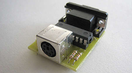
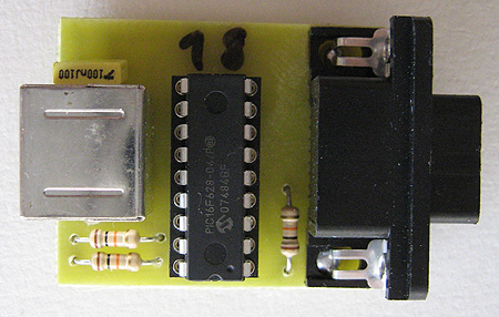
Ce circuit de taille réduite permet de connecter de façon transparente une souris ps/2 à un ordinateur Amiga ou Atari ST. Il détecte automatiquement chacune de ces deux machines afin d'envoyer les signaux correspondants.

(merci à Arklif pour les photos)

Une version utilisable sur les ordinateurs Thomson TO est également disponible.

Une version du circuit spécialement adaptée pour recevoir une alimentation 5v externe est disponible. Elle permet d'utiliser une souris optique qui consomme trop d'électricité par rapport à ce que le port souris d'un amiga peut fournir.

Ce montage est adapté de celui disponible ici.

Informations techniques : le montage est réalisé autour d'un PIC 16f628 et comporte très peu de composants : 3 résistances et un condensateur.

Voici le schéma du circuit (résolution 300 dpi), et le projet piklab contenant le code source en assembleur.

Projet piklab Projet eagle

Prix : 20 euros, expédition comprise

ATTENTION : Problème de détection Atari/Amiga

certains utilisateurs sur Amiga 1200 et 4000 se sont apperçus que l'adaptateur se croyait sur Atari au démarrage de la machine. Cela est probablement du à de mauvaises valeurs de composants.

Il existe hereusement une solution simple pour forcer le mode Amiga : il suffit de couper une piste de l'adaptateur comme suit.

couper la piste entre la broche 6 du PIC et la resistance.

Dans ce cas, l'adaptateur fonctionnera toujours en mode Amiga et ne pourra pas être utilisé sur un Atari.

Des trucs AVR

Posted by pulkomandy on Mon Oct 18 22:36:51 2010  •  Comments (0)  • 

Je n'avais pas encore mis de news ici, mais les adaptateurs clavier amiga fonctionnent et sont en vente au prix de 20€. Contrairement à AmiPS/2, Amikey2USB est vendu avec un boîtier.

Comme les Atmel AVR marchent plutôt bien, j'en ai profité pour faire aussi une version ps/2 vers usb de l'adaptateur, ainsi qu'une carte pour gérer des boutons dans une borne d'arcade (encore en prototype pour l'instant).

En tout cas, je n'ai pas toujours le temps de maintenir ce site à jour, et j'utilise maintenant mon installation de Trac. Il y a donc d'autres façons de me surveiller...

  • La liste des projets. Pour l'instant tout ce qui est électronique est dans le projet avrstuff. Mais d'autres pourraient apparaitre.
  • Les flux RSS: ils sont également disponibles dans chaque projet de Trac, mais je trouve ça plus pratique d'avoir une page avec un apperçu complet.

D'autres projets sont en cours, mais je vous en dirai plus seulement une fois que ça commencera à fonctionner.

News en vrac

Posted by pulkomandy on Mon Feb 22 21:55:11 2010  •  Comments (0)  • 

Bon, il n'y a pas eu de mises à jour dans ce coin depuis un certain temps, donc en voilà quelques unes...

  • J'ai enfin fini de souder mon USBasp. Ce programmeur permet de graver des puces atmel AVR. Ça me changera un peu des PICs qui ont un assembleur assez illisibles et ne sont pas trop fait pour le C...
  • Ce programmeur va me permettre de travailler sur l'adaptateur permettant de brancher un clavier amiga (4000 ou 2000) sur une machine en USB. Mais j'ai fait quelques erreurs de gravure de la carte qu'il va falloir rattraper.
  • La version interne de l'AmiPS2 est maintenant officiellement disponible. Même prix que la version externe, légèrement plus petite, et avec deux trous de fixation pour l'accrocher ou vous voulez.
  • Prochaine étape : construire un programmeur de CPLD qui va me servir entre autres, pour le projet ReACID. Mais aussi par exemple pour fabriquer des UltraSatan ou d'autres machins un peu compliqués dans ce genre.

Cela dit, je suis assez pris par les projets scolaires, donc tout ça ne sera pas fini "la semaine prochaine". Plutôt pendant l'été. Les AMIps2 sont toujours disponibles (il en reste aussi quelques uns en version externe). Le reste arrivera petit à petit.

Lecteur de disquettes Floppy-1 pour Amstrad CPC et Amstrad Plus

Posted by pulkomandy on Mon Jul 6 14:06:19 2009  •  Comments (0)  • 

Floppy-1

photo du Floppy-1

Un lecteur de disquette pour les ordinateurs Amstrad CPC(+).

Vrai signal "ready", switchs de changement de face et de forçage en A, alimentation 5v externe.

3 versions avec des connecteurs différents : CPC Old, CPC Old Centronics, CPC Plus.

45 euros, expédition comprise

Adaptateur joystick 4joy pour Amiga

Posted by pulkomandy on Mon Jul 6 14:04:33 2009  •  Comments (0)  • 

4Joy

Cet adaptateur permet de connecter deux joysticks supplémentaires sur le port parallèle de votre Amiga.

Il est utilisable avec les jeux suivants :

  • Dynablaster
  • Gauntlet II (US Gold)
  • International Soccer (Microdeal)
  • Kick Off II (Anco)
  • Knock Out 2
  • Leatherneck (Microdeal)
  • Projectyle (Electronic Arts)
  • TV Sports Basketball (Cinemaware)

L'adaptateur coûte 15 euros, expédition incluse.

Afficheur a LEDs ledmeter pour tout ordinateur equipe d'un port parallele

Posted by pulkomandy on Mon Jul 6 14:01:55 2009  •  Comments (0)  • 

LEDMeter-2

ledmeter ledmeter ledmeter ledmeter ledmeter

Brochage du connecteur CON1:

  • 1: Data 4
  • 2: Masse
  • 3: Data 3
  • 4: Data 2
  • 5: Data 1
  • 6: Data 0

Le ledmeter est constitué de 32 DELs et se connecte sur le port parallèle de n'importe quel PC. Le circuit est plutôt simple puisqu'il s'agit simplement de démultiplexeurs (et d'une porte NON). Ceci permet une programmation également très simple: pour allumer une DEL, il suffit d'envoyer son numéro sur le port parallèle. En théorie, il est possible de cabler jusqu'à 2565 diodes sur un port parallèle. Cependant ma version n'en comporte que 32 pour des raisons de place disponible.

Une petite vidéo de démonstration est disponible ici.

Vous pouvez télécharger le projet eagle et le code source du programme pour linux.

Si vous voulez construire une version de ce ledmeter, si vous améliorez le programme, merci de partager vos idées et de m'envoyer des photos de vos créations.

ZenBox : 2 lignes, 1 telephone

Posted by pulkomandy on Fri Jun 27 23:12:37 2008  •  Comments (0)  • 

Zen PhoneBox

Il s'agit d'un boîtier permettant d'utiliser deux lignes teléphoniques (dans notre cas une ligne freebox et une ligne france téléom) avec un seul téléphone. Le circuit a été conçu par VieuxGeo, vous pouvez avoir pas mal d'infos sur son site: ICI